Christophe Fouquet, CEO of ASML, the world’s only supplier of extreme ultraviolet (EUV) lithography equipment for chip production, visited Korea this week to attend the opening ceremony of ASML Korea’s new headquarters in Hwaseong, Gyeonggi, and to seek stronger partnerships with major Korean semiconductor companies.
This marks Fouquet’s first official visit to Korea since taking office in April 2024, signaling his intention to reinforce cooperation with key clients such as Samsung Electronics and SK hynix.
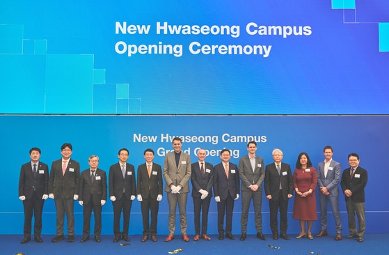
ASML held the opening ceremony for its new “Hwaseong Campus” in Song-dong, Hwaseong, on Wednesday. The event was attended by about 80 people, including Samsung Electronics Device Solutions division CTO Song Jai-hyuk, SK hynix President Cha Seon-yong, executives from ASML’s client companies, officials from the Dutch Embassy in Seoul and representatives from the Korean government and local authorities. From the government, Kang Kam-chan, director-general for trade and investment at the Ministry of Trade, Industry and Energy, was present.
ASML is the exclusive manufacturer of EUV lithography equipment, essential for advanced semiconductor production. While it is technically a supplier to global chipmakers such as Samsung Electronics, SK hynix and TSMC, its irreplaceable position in the supply chain has earned it the nickname “super-subcontractor” in the industry.
At the ceremony, Fouquet emphasized that establishing a campus in Hwaseong was a highly strategic decision. He said the new Hwaseong Campus symbolizes ASML’s commitment to trust, innovation, sustainability and growth with its Korean customers.
Fouquet added that locating the company in Hwaseong, where major semiconductor manufacturers operate, allows closer collaboration and faster technical support. Fouquet noted that as semiconductor manufacturing becomes increasingly complex, this proximity will also help facilitate efficient technology transfer.
ASML invested 240 billion won ($163.8 million) in the new campus, which consists of two buildings: Building A, 11 stories above ground and four below, and Building B, five stories above ground and four below. Building A houses the main offices, while Building B contains a Repair & Reuse (R&R) Center and a training center.
The company is in the process of relocating its staff and equipment from nearby sites. Around 1,500 employees are expected to work at the new facility by the end of the year.
The new complex will serve as more than an office space but an integrated hub for equipment maintenance, repair and customer training. The R&R Center will handle repairs and part reuse for lithography machines used by Samsung Electronics and SK hynix, helping to reduce costs, shorten turnaround times and strengthen supply chain stability.
The training center is equipped with both deep ultraviolet (DUV) and EUV lithography systems, offering hands-on programs for semiconductor engineers to better understand new technologies and enhance their operational capabilities. The center plans to host around 2,000 trainees annually across more than 100 programs, and will eventually offer courses on next-generation high numerical aperture EUV systems.
Before and after the event, Fouquet met with top executives from Samsung Electronics and SK hynix. Industry sources said that after the opening ceremony on Wednesday, Fouquet visited Samsung’s DSR Tower in Hwaseong for a luncheon with Vice Chairman Jun Young-hyun and CTO Song. On Tuesday, Fouquet reportedly met with SK hynix CEO Kwak Noh-jung.
Industry insiders are watching closely to see whether Fouquet’s visit will accelerate the stalled plan to establish a joint R&D center with Samsung Electronics. The two companies signed an MOU in 2022 to build a 1.2-trillion-won research and development facility, but the project has made little progress since.
This article was originally written in Korean and translated by a bilingual reporter with the help of generative AI tools. It was then edited by a native English-speaking editor. All AI-assisted translations are reviewed and refined by our newsroom.
댓글목록
등록된 댓글이 없습니다.